Material components of electronics are a fundamental part of the manufacturing of small devices. The miniaturization trend in electronic devices extends to the point of molecular-scale functionality in the nanometer scale. To stay in this road manufacturers require materials that can also be an integral part of the device, having several functions.
Nowadays, advances in nanotechnology have allowed the production of nano-arrays and morphologies of materials. However, the necessity of simple fabrication methods of two and three-dimensional ordered structures remains.
Metal-Organic Frameworks (MOFs for short) are a unique kind of nanoporous material combining rigid characteristics of inorganic compounds and the flexibility of organic linkers. In the manufacturing of electronic devices, MOFs have opened new ways to overcome issues of conventional materials.
Some of the advantages of MOFs are:
- Well-defined pore size and structure – Gives the ability to understand atomic interactions.
- Pore shape manipulation – Offer a rational template design based on atomic interactions.
- Physical and chemical tunability – Since the components of the structures can be chosen, properties like electrical, optical, and mechanical can be easily manipulated.
- High porosity – Allows the addition of guest molecules to modify or add physical or chemical properties.
Most known MOFs are dielectrics (electrical isolators) but others with attractive properties like semiconductors, magnetic, ion conductivity, and luminescence are also available. Each type of these MOFs can have different functions in electronic devices. In the following sections, we describe their most common applications.
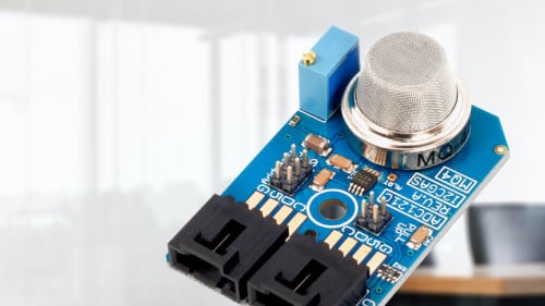
Sensors
One of the strongest features of MOFs is that they can be synthesized to have high specificity towards chemical compounds of interest. Therefore, its application in sensor technology provides high sensitivity and selectivity to the device.
The chemical interaction of the MOF structures with an analyte can result in changes of a physical property like temperature or pressure, which can be used as a signal for detection. For instance, a molecule absorbed in a MOF can generate structure swelling. When this process is generated in a thin film attached to a microcantilever gives as a result an electromechanical sensor. In this example, the MOF participates as a non-electronic element, other possible roles are as a passive electronic element, active electronic element, and as a scaffolding element.

Energy storage devices
Ion conductors in energy storage devices like batteries, supercapacitors, and fuel cells are key elements to achieve high performance. In the field of Li-ion batteries, there is a search for non-liquid electrolytes aiming to lower the risk of flammability while keeping storage capacity. Some promising results have been obtained in the application of MOFs like MOF-74 and UiO-66 for the fabrication of dry free-flowing powder with ion conductivity comparable with that of organic polymer solid electrolytes (0.012-0.018 mS/cm).
Another application of MOF materials is found in the field of supercapacitors. In the supercapacitor technology, the electrode material requires a high specific surface area and enhanced conductivity. In the fabrication of these devices, MOFs are used in a modified version or in combination with other materials to enhance their electric conductivity. MOFs made up of metals such as Ni, Co, Cu, Mn, Cr, Zr, Fe, and Zn in combination with organic ligands have been investigated for such applications. The specific capacitance of MOF-based materials ranges from 200 to 1600 F/g.
The most prominent example of MOFs in such supercapacitors is probably the cooperation of our scientific advisor Mircea Dinca from the MIT and Lamborghini.
 Photovoltaics
A photovoltaic cell usually consists of three elements: charge collecting electrodes, charge-transporting layers, and a photoactive material. The most straightforward application of MOFs in photovoltaic cells is as photoactive materials due to their semiconducting properties. Owing to the facile manipulation of the chemical composition of MOFs, the bandgap energy can be tuned for enhanced performance of these materials as semiconductors.
Other variants of these devices such as dye-sensitized solar cells (DSSCs) can incorporate MOF materials as photoanode and counter-electrode materials involving semiconducting and charge transfer properties as well as electrocatalytic activity.
 Light-emitting devices
Metal-Organic Frameworks can be fabricated to have light emission properties like luminescence, such properties can be incorporated either in one of the constituents of the structure (metal nodes or organic linkers) or with a guest molecule (i.e. lanthanide ions) in a post-synthesis modification. These types of MOFs can be used as phosphors in light-emitting diodes (LEDs), having the ability to fine-tune the emission color temperature by changing the chemical nature of its components.
Conclusions
Metal-Organic Frameworks offer several advantages in the fabrication of electronic devices. These advantages are the result of the ability to realize a rational design of the MOFs structures. MOF properties can be tailored in terms of pore size and chemical functionality. The tunable responses and switching properties upon external perturbations like temperature, pressure, radiation, magnetic field, electric potential, acoustic waves, chemical environment, etc. allow the application of MOF-based materials in a wide variety of electronic devices.